1. U.S. Export Control
In recent years, the semiconductor industry has been at the forefront of rising geopolitical tensions between the U.S. and China. As the U.S. broadens restrictions on exports of certain semiconductors and semiconductor manufacturing equipment (SME) to China, it is increasingly important that semiconductor companies doing business in China stay informed of changing export control laws and be able to quickly implement effective compliance measures.
While compliance with export control laws is critical to avoid significant legal and financial penalties, loss of privileges, and reputational harm, a more proactive strategy may be needed when reactive compliance alone can lead to catastrophic losses in revenue. This article reviews a proactive strategy we used to enable our client to resume development and production of advanced dynamic random-access memory (DRAM) integrated circuits (ICs) that had been entirely halted by recent U.S. export controls. The strategy also helped to alleviate billion-dollar losses in the broader U.S. SME segment that resulted from the most expansive export control action in decades.1 This case study does not include follow-up and on-going work in this area.
2. October 7, 2022 IFR
The U.S. Bureau of Industry and Security (BIS) issued an interim final rule (IFR) on October 7, 2022 (hereafter “2022 IFR”) that essentially prohibited the export of items used in the development or production of ICs at facilities in China that fabricate certain logic ICs, NOT AND (NAND) memory ICs, or DRAM ICs. Specifically, the 2022 IFR prohibited certain exports relating to any of the following criteria2:
(A) Logic ICs using a nonplanar transistor architecture or with a production technology node of 16/14 nanometers or less;
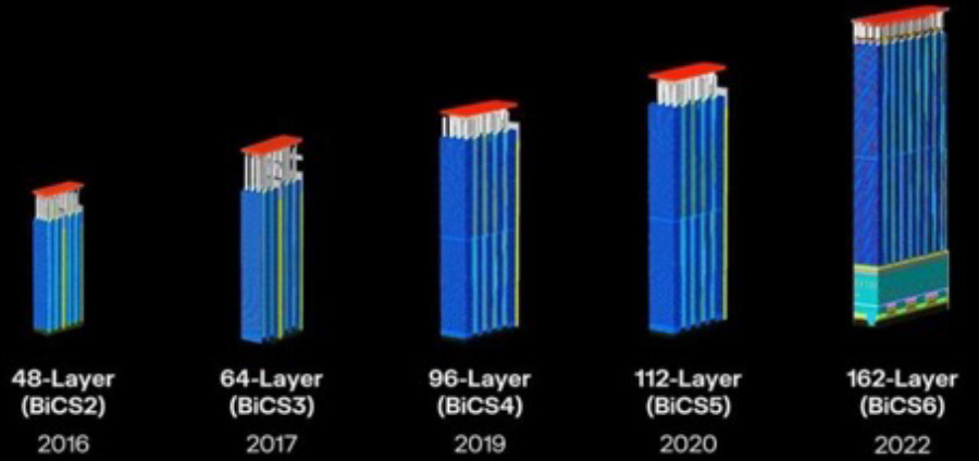
(B) NAND memory ICs with 128 layers or more; or
(C) DRAM ICs using a production technology node of 18 nanometer half-pitch or less.
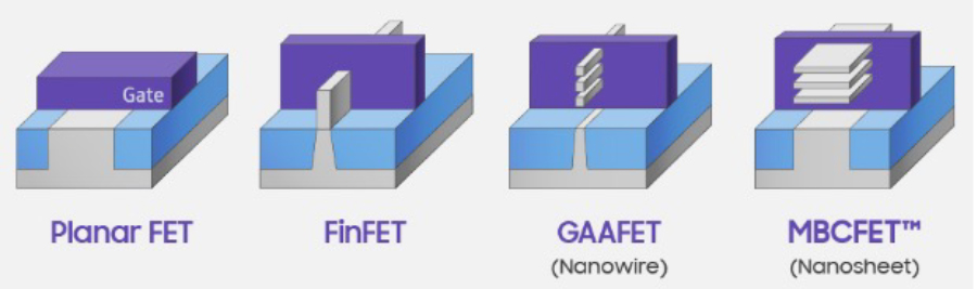
Put simply, the 2022 IFR prevented U.S. companies from exporting SME to China that would be used in any facility where advanced logic, NAND memory, and DRAM ICs would be developed or produced, regardless of whether the equipment would actually be used to develop or produce those advanced ICs. FIG. 1 below shows examples of (a) nonplanar transistor architectures, (b) multilayer NAND memory architectures, and (c) DRAM cell architectures.
|
(A) Planar and nonplanar transistor architectures for logic ICs3
|
|
(B) Multi-layer NAND architectures for NAND memory ICs4
|
|
(C) Memory-cell architectures for DRAM ICs5 FIG. 1: Examples of circuit architectures of different types of ICs |
3. U.S. SME Segment
Revenues for the U.S. semiconductor industry in 2021 were $256 billion,6 with $43 billion attributed to the SME segment7, 8. Three of the world’s largest SME companies are headquartered in the U.S. and account for 42% of the global SME market9— Applied Materials, Lam Research, and KLA Corp. These companies typically earn approximately 90% of their revenue from sales outside the United States, e.g., from exported items,10 with about 30% attributed to China11.
- Applied Materials (NASDAQ: AMAT) specializes in equipment, services, and software for production of ICs, flat-panel displays, and advanced materials, with a focus on deposition, etching, and inspection technologies. Total revenues in 2021 were $24 billion,12 with an average of 32%13 of revenues from China preceding the 2022 IFR.
- Lam Research (NASDAQ: LRCX) is a prominent global provider of wafer fabrication equipment and services used in the semiconductor industry, specializing in etch, deposition, and clean technologies critical to advanced semiconductor manufacturing. Total revenues in 2021 were $17 billion,14 with an average of 32%15 of revenues from China preceding the 2022 IFR.
- KLA Corp. (NASDAQ: KLAC) is a leading provider of process control and yield management solutions for the semiconductor and related industries, offering advanced inspection, metrology, and analytical systems used in semiconductor manufacturing. Total revenues in 2021 were $8 billion,16 with an average of 28%17of revenues were from China preceding the 2022 IFR.
FIG. 2 below shows a breakdown of revenues of the three major U.S. SME companies just prior to the 2022 IFR.
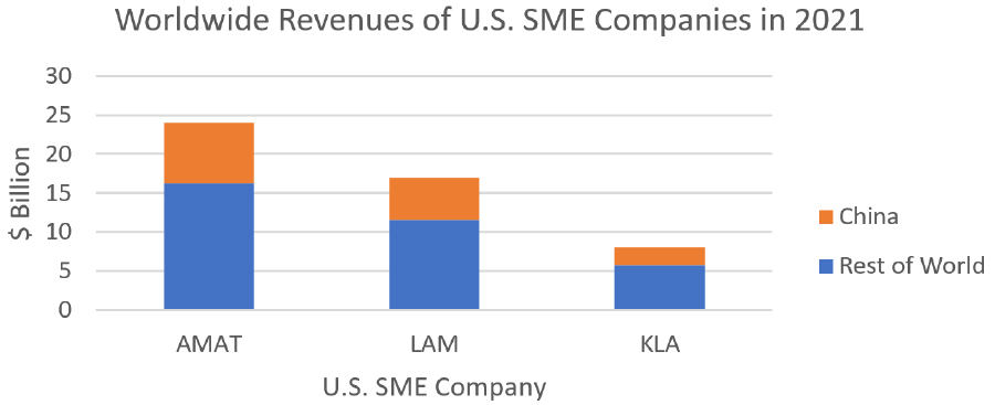
FIG. 2: Comparison of revenues from China and Rest of World for U.S. SME companies
4. Collateral Damage
The 2022 IFR intended to protect U.S. national security interests by hindering China’s military modernization and surveillance efforts, and it sought to prevent China from undercutting U.S. technology leadership or unduly interfering with commercial trade.18 However, the 2022 IFR directly affected many U.S. semiconductor segments, including SME, supercomputing, military/aerospace, and materials. The $43 billion U.S. SME segment, which is nearly four times larger than any other U.S. semiconductor manufacturing industry,19 was hit hard. For comparison, marginal impacts of the 2022 IFR on the supercomputing, military/aerospace, and materials segments are indicated below.
- Supercomputing.The global market of supercomputers was just $6.5 billion in 2021 (with just 21% from the U.S.).20 A specific dollar amount of exports to China is unknown but generally understood to be negligible due to existing strict national-defense export laws.
- Military/aerospace. The global market of military/aerospace was just $6.3 billion in 2021 (with an unknown but majority percentage directed for use by U.S. military)21. A specific dollar amount of exports to China is unknown but generally understood to be negligible due to existing strict national-defense export laws.
- Materials. The U.S. semiconductor materials segment is much smaller than the U.S. SME segment—at $15 billion22 in 2021 compared to $43 billion—and it accounts for just 20% of the global market23.
Returning to the U.S. SME segment, the three largest U.S. SME companies each derived approximately 30% of their respective total revenues from China prior to the 2022 IFR,24 but those percentages drastically declined leading up to and following the 2022 IFR. Specifically, Applied Materials’ China revenue dropped 14% (from 32%25 to 18%26), Lam Research’s China revenue dropped 8% (from 32%27 to 24%28), and KLA Corp’s China revenue dropped 5% (from 28%29 to 23%30). These declines amounted to a roughly a billion dollars lost from the U.S. SME segment per quarter, as indicated by the graph of quarterly China revenues shown in FIG. 3 below.31
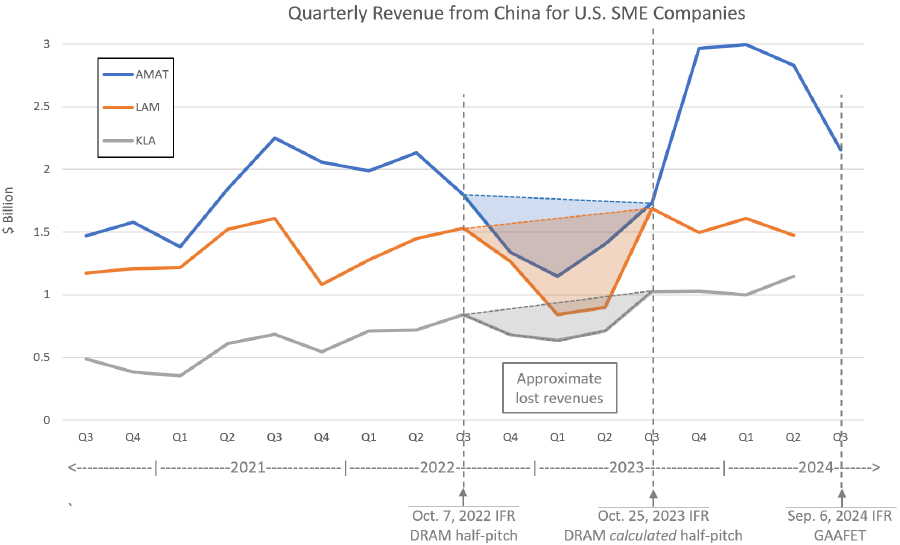
FIG. 3: Lost revenues resulting from the 2022 IFR
5. Logic v. Memory ICs
While the 2022 IFR restricted exports of SME and semiconductor manufacturing materials for logic ICs and memory ICs (i.e., NAND and DRAM), the latter caused most of the revenue loss to the U.S. SME segment. Regarding logic ICs, China’s manufacturing capabilities lagged significantly behind the 16/14 nm production technology node indicated by the 2022 IFR.32 Consequently, U.S. SME companies could continue selling equipment to China for developing and/or producing logic ICs using the less advanced production technology nodes prevalent there at the time. The situation for manufacturing of NAND memory ICs and DRAM ICs can be divided into two groups: (a) international companies with manufacturing facilities in China; and (b) China-based companies.
(a) International companies. IC memory manufacturing is dominated by three companies: Samsung Electronics (headquartered in South Korea), SK Hynix (headquartered in South Korea), and Micron Technology (headquartered in the U.S.), which together accounted for 95% of all global DRAM IC revenues and 67% of all global NAND memory IC revenues in 2020.33 Samsung Electronics and SK Hynix both operated large manufacturing facilities in China in 2021 and 2022, while Micron did not. For example, Samsung Electronic’s Xi’an, China plant accounted for about 40% of its global NAND IC production in 2021, and SK Hynix’s Wuxi, China plant accounted for about 48% of its global DRAM IC production in 2021.34 However, Samsung Electronics and SK Hynix received one-year exemptions to the 2022 IFR that allowed them to continue development and production of advanced memory ICs, which were extended indefinitely in October 2023 (subject to reviews).35
(b) China-based companies. By 2022, leading Chinese manufacturers of NAND memory ICs, such as Yangtze Memory Technologies Corp (YMTC), were reported to be developing 128-layer (or more) NAND memory ICs as identified in the 2022 IFR. Similarly, by 2022, leading Chinese manufacturers of DRAM ICs, such as ChangXin Memory Technologies (CXMT), were reported to be developing 18-nm half-pitch (or less) DRAM ICs as identified in the 2022 IFR. Consequently, the 2022 IFR directly affected the ability of these companies to purchase the SME they needed to develop and subsequently produce these advanced ICs. Without some sort of relief, these companies were at risk of faltering.
6. Clarify the Text
As indicated above, indiscriminate compliance to the text of the 2022 IFR was not a viable option for China-based companies manufacturing memory ICs that wanted to remain competitive at best or merely solvent at worst. Our task was to figure out how to comply with the 2022 IFR while simultaneously enabling the client, a DRAM manufacturer, to continue developing its advanced DRAM ICs.
We scrutinized the language of the 2022 IFR for any loopholes or ambiguities that could help. An operative portion of the 2022 IFR is reproduced below. Under the revised § 744.6 of the Export Administration Regulations (EAR), no U.S. Person may, without a license from the BIS, perform the activities of:
(c)(2)(i) Shipping, transmitting, or transferring (in-country) to or within the PRC36 any item not subject to the EAR that you [(the U.S. Person)] know will be used in the “development” or “production” of integrated circuits at a semiconductor fabrication “facility” located in the PRC that fabricates integrated circuits meeting any of the following criteria:
(A) Logic integrated circuits using a nonplanar transistor architecture or with a “production” technology
node of 16/14 nanometers or less;
(B) NOT AND (NAND) memory integrated circuits with 128 layers or more; or
(C) Dynamic random-access memory (DRAM) integrated circuits using a “production” technology node
of 18 nanometer half-pitch or less.37
Several approaches to narrow the language of the 2022 IFR are indicated below, which we ultimately deemed unproductive.
- U.S. Persons. The 2022 IFR describes prohibitions on the export of items by “U.S. Persons.” While EAR § 772.1 provides a broad definition, the BIS clarified in its October 28, 2022 FAQ that, for purposes of this rule, a U.S. Person is essentially any person in the United States and any juridical person organized under U.S. laws, e.g., a corporation.38
- Semiconductor fabrication facility. The 2022 IFR uses the term “semiconductor fabrication facility” without defining what “facility” means. The BIS clarified in its October 28, 2022 FAQ that the definition provided in EAR § 772.1 controls, where each building of a campus may be considered a separate facility.39 Thus, according to the 2022 IFR, a U.S. Person cannot export to China any items that will be used in the same building (located in China) where any category A (logic), B (NAND), or C (DRAM) ICs are produced or developed, regardless of whether those items are actually used in the production or development of the category A, B, or C ICs in that building.
- Development; production. The 2022 IFR uses the terms “development” and “production” without formal definitions. The BIS did not provide clarification on these terms at the time, so it was reasonable to assume that the definitions provided in EAR § 772.1 control. In short, “development” is related to all stages prior to serial production, and “production” means all production stages (see EAR § 772.1 for lists of examples of each).
7. Clarify the Technology
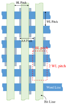
Instead of narrowing the language of the 2022 IFR, we determined the best approach was to clarify the definition of the regulated technology. Specifically, what does “a production technology node of 18 nanometer half-pitch or less” mean, exactly? It turns out DRAM “half-pitch” can be interpreted in several ways—M1 half-pitch, active area half-pitch, and calculated half-pitch—and their values can vary significantly. A pitch is a distance between equivalent points on adjacent repeating elements (like a center-to-center distance), and a half-pitch is simply half of the pitch.
- M1 half-pitch. Half the center-to-center distance between M1 interconnects of a memory cell. M1 is the lowest metal interconnect layer and is almost always used for the bitlines of a DRAM cell. Bitlines are interconnects that carry data, as opposed to wordlines that carry control signals.
- Active area half-pitch. Half the center-to-center distance between the active areas, or bodies, of memory cells in a direction perpendicular to the long axis of the elongated active areas. The active area is where the transistor of the ubiquitous 1-transistor, 1-capacitor (1T1C) DRAM memory cell is formed.
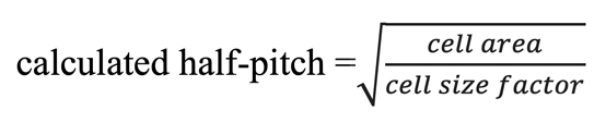
- Calculated half-pitch. The memory cell area divided by the cell size factor, raised to the one-half power, i.e.,
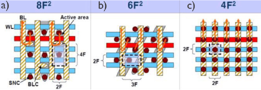
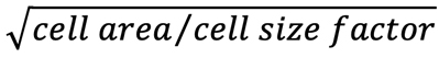 . The cell size factor is a normalized area based on a generalized feature size, F. For example, the cell size factor is 8 for an 8F2 memory cell architecture, 6 for 6F2, and so on.40,41 More about memory-cell architectures later.
FIG. 4 below depicts a typical DRAM cell showing the bitlines (vertical), the wordlines (horizontal), and the active areas (diagonal).
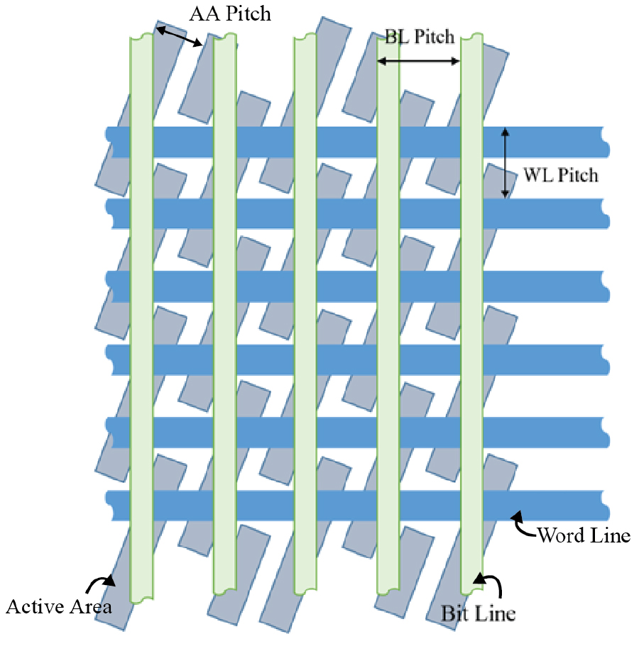
FIG 4: DRAM cell showing bitline (BL), active area (AA), and wordline (WL) pitches
8. Clarify the Purpose
In the semiconductor industry, a technology node refers to a specific semiconductor manufacturing generation and its design rules, and it indicates the scaling of integrated circuits from one generation to the next. Scaling can refer to almost any parameter or metric of interest, but almost always refers to storage density (e.g., bits per square millimeter) for memory ICs and circuit speed for logic ICs (e.g., clock frequency). A technology node was historically expressed in terms of microns or nanometers (e.g., 0.13 µm, 90 nm, etc.), and it correlated to some tiny, fabricated feature of an IC like M1 half-pitch for DRAM ICs or transistor gate-length for logic ICs.
As indicated above, DRAM M1 half-pitch is half the center-to-center distance between the lowest metal layer of a memory cell, i.e., M1 interconnects. In the early days of semiconductors, this definition worked well in describing the scaling between DRAM technology nodes because M1 half-pitch consistently and predictably scaled (i.e., shrank) with each subsequent generation, and it correlated well with storage density. In fact, by 1999, DRAM M1 half-pitch was declared by the International Technology Roadmap for Semiconductors (ITRS)42 to be the standard way to designate DRAM technology nodes.43
But the usefulness of M1 half-pitch to define DRAM technology nodes was short-lived due to a disappearing correlation between M1 half-pitch and the chosen micron or nanometer number designating a technology node.44 This is partly the reason why seemingly arbitrary alphanumeric and Greek letters are commonly used to describe today’s technology nodes (e.g., 1α, 1β, etc.).
To be clear, the key aspect of a designator for a technology node is not some tenuous connection to a fabricated feature size like DRAM M1 half-pitch, but its ability to accurately indicate the scaling between semiconductor technology nodes. This was emphasized in the 2005 ITRS, which stated:
[W]e no longer use the term “technology node.” Instead, each distinct scaling feature is specifically referenced as such. Note that, for some degree of continuity, we are still showing DRAM M1 half-pitch at the top of many tables, but it is no longer described as the measure of “technology node.” It is just one among several historical indicators of IC scaling.45
Accordingly, the half-pitch referred to in the 2022 IFR should faithfully indicate technology-node scaling, because a half-pitch that fails to do so could lead to ambiguous application of the 2022 IFR—and potentially excessive economic damage to the U.S. SME industry.
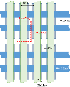
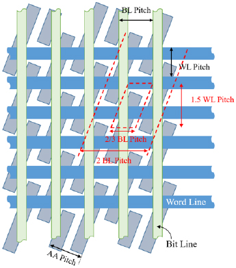
Notwithstanding that the semiconductor industry had long since abandoned M1 half-pitch as the designator for technology nodes,46 M1 half-pitch could be ruled out with a simple technical argument. Practically all DRAM memory cells today utilize a 6F2 architecture. One (older) version of the 6F2 architecture (referred to as 2×3) comprises wordlines oriented perpendicular and above elongated active areas, and bitlines oriented colinear with the active areas and above the wordlines, as shown in FIG. 5(B) below. Another (newer) version of the 6F2 architecture (referred to as 3×2) comprises the same layering and same bitline (M1) pitch as the older 2×3, but the elongated active areas are staggered and slanted at an angle with respect to the bitlines, as shown in FIG. 5(C) below. This purely geometric maneuver allows the wordlines to be brought closer to each other, thereby reducing the memory cell area without reducing the bitline pitch, i.e., without reducing the M1 half-pitch. In other words, the storage density—the key scaling metric for designating DRAM technology nodes—is independent of M1 half-pitch. Thus, M1 half-pitch does not faithfully indicate technology-node scaling.
 |
 |
 |
| (A) 8F2 DRAM cell | (B) 2×3 6F2 DRAM cell | (C) 3×2 6F2 DRAM cell |
| FIG 5: DRAM cell architectures showing different cell areas | ||
A similar argument could be made to rule out active area half-pitch. The 8F2 “folded bitline” architecture was mainstream until approximately 2008 when it was supplanted by the 2×3 6F2 “open bitline” architecture.47 In the 8F2 architecture, showin in FIG. 5(A) above, the elongated active areas are staggered along their long axes so that a given wordline contacts only odd or only even active areas in the memory array. In contrast, in the 2×3 6F2 architecture, the ends of the elongated active areas are aligned so that a given wordline contacts both odd and even active areas in the memory array. However, in both architectures, the wordlines are oriented perpendicular and above elongated active areas, and bitlines are oriented colinear with the active areas and above the wordlines. Thus, for the same active area half-pitch, the 8F2architecture has a normalized area of 8 and the 6F2 architecture has a normalized area of 6. This is a 25% reduction in memory cell size yielding a 33% improvement in storage density48—the key scaling metric for designating DRAM technology nodes—that is achieved by architectural improvements independent of active area half-pitch. Thus, active area half-pitch does not faithfully indicate technology-node scaling.
The industry has been working toward a 4F2 architecture for several decades, but additional semiconductor manufacturing advancements are required, such as those concerning vertical transistor structures, high-κ dielectrics, and so on.49 There are two implications. First, parallel to the argument above, the scaling in storage density by transitioning from 6F2to 4F2 is due to architectural improvements independent of the active area half-pitch. Second, the transition from 6F2 to 4F2 will occur at some future technology node that encompasses the required additional semiconductor manufacturing advancements that have practically nothing to do with patterning a smaller active area onto a silicon substrate. For these additional reasons, active area half-pitch does not faithfully indicate technology-node scaling.
That leaves calculated half-pitch as the best interpretation of “half-pitch” in the 2022 IFR. One argument could be made based entirely on the semiconductor industry’s consensus on redefining DRAM half-pitch from M1 half-pitch to calculated half-pitch according to the 2017 International Roadmap for Devices and Systems (IDRS):
The definition of DRAM Half pitch has been changed from this edition. Because of 6F2 DRAM cell, BL pitch is no more critical dimension. . . . Calculated half pitch is use [sic] the following equation “Calculated half pitch= (Cell Area/ Call [sic] size factor)^0.5.”50
However, a better argument was to show that calculated half-pitch faithfully indicates technology-node scaling. To repeat, calculated half-pitch is defined as ![]() .51 Cell area accounts for process-related changes in any relevant feature sizes—such as bitline pitch, wordline pitch, and active area pitch—as well changes due to geometric maneuvering, such as staggering and slanting the active areas. Further, cell size factor accounts for changes in memory cell architecture, such as the evolution from 8F2 to 6F2 and eventually to 4F2. In this manner, calculated half-pitch faithfully indicates storage density, which is the key scaling metric for designating DRAM technology nodes. Consequently, it is reasonable to interpret category C the 2022 IFR as DRAM ICs using “a ‘production’ technology node of 18 nanometer calculatedhalf-pitch or less.”
.51 Cell area accounts for process-related changes in any relevant feature sizes—such as bitline pitch, wordline pitch, and active area pitch—as well changes due to geometric maneuvering, such as staggering and slanting the active areas. Further, cell size factor accounts for changes in memory cell architecture, such as the evolution from 8F2 to 6F2 and eventually to 4F2. In this manner, calculated half-pitch faithfully indicates storage density, which is the key scaling metric for designating DRAM technology nodes. Consequently, it is reasonable to interpret category C the 2022 IFR as DRAM ICs using “a ‘production’ technology node of 18 nanometer calculatedhalf-pitch or less.”
9. Draft Mutually Beneficial Opinions
While distinctions between various half-pitches may seem arbitrary or confusing, they were critically important to determining whether U.S. SME companies could legally export advanced SME to China-based manufacturers of advanced ICs. As indicated above, DRAM half-pitch historically referred to the smallest feature size in the memory cell. In the ubiquitous 3×2 6F2 architecture, that is typically the active area pitch because of staggering and slanting the active areas. But, as explained above, active area half pitch does not faithfully represent memory-cell size across architectures, so that interpretation of “half-pitch” can result in inaccurate application of the 2022 IFR. Further, calculated half-pitch—which does faithfully represent memory-cell size across architectures—is typically larger than active area half-pitch for the 3×2 6F2 architecture. Thus, interpreting “half-pitch” as calculated half-pitch was a win for U.S. SME companies because it enabled objective and accurate compliance with the 2022 IFR, and it was a win for the China-based DRAM manufacturers because it enabled them to manufacture advanced DRAM ICs that would otherwise not be possible.
We drafted legal opinions based on the preceding material to guide U.S. SME companies in accurately interpreting the 2022 IFR with respect to the development and production of advanced DRAM ICs. We also drafted legal opinions that included semiconductor metrology data of actual DRAM ICs produced by our client showing a calculated half-pitch greater than 18 nm. Through the first couple quarters of 2023 we continued to advance our calculated half-pitch interpretation, and we obtained additional third-party semiconductor metrology data to assure the U.S. SME companies that any SME exported to our client’s facilities would be in compliance with the 2022 IFR. At least several U.S. SME companies consulted with the BIS for further assurances, and by mid-2023, it appeared our strategy had been successful. Indeed, On October 25, 2023, the BIS issued a new IFR (hereafter “2023 IFR”) that formally adopted our interpretation of half-pitch in the 2022 IFR as calculated half-pitch, the text of which is reproduced below (emphasis added).52
Technical Note to definition of “Advanced-Node Integrated Circuits”:
For the purposes of paragraph (3) of this definition, the calculation methodology to be used in determining whether a DRAM integrated circuit uses a production technology node of 18 nanometer half-pitch or less is the calculated half-pitch method developed, adopted, and used by the Institute of Electrical and Electronics Engineers (IEEE) and published in the International Roadmap for Devices and Systems (IRDS), as follows:
Cell size factor is 8, 6 or 4 depending on the DRAM architectures. Cell area is defined as Wordline*Bitline (which takes into consideration both transistor and capacitor dimensions)[.]
10. Conclusion
As indicated in the graph of quarterly revenues of U.S. SME companies shown in FIG. 3 above, the U.S. SME companies had begun exporting advanced SME to China-based semiconductor manufacturing companies well before issuance of the 2023 IFR. Our proactive strategy for the 2022 IFR not only helped to revive our client’s competitiveness in the global DRAM IC market, but it helped to alleviate the billion-dollar losses incurred by the U.S. SME companies.
Click here to download this article.
1 “A Seismic Shift: The New U.S. Semiconductor Export Controls and the Implications for U.S. Firms, Allies, and the Innovation Ecosystem,” S. Shivakumar, et al., Center for Strategic & International Studies (Nov. 14, 2022). Retrieved Dec. 25, 2024 from link.
2 Interim Final Rule 87 FR 62186, United States Federal Register, vol. 87, no. 197, pp. 62186-62215.
3 “GAA Structure Transistors,” Samsung (Nov. 20, 2019). Retrieved Dec. 24, 2024 from link.
4 “Western Digital to produce 162-Layer NAND before the end of the year,” Wccftech (May 17, 2022). Retrieved Dec. 24, 2024 from link.
5 “From Transistors to a Complete System in Package – The 3D Evolution in Semiconductors’ Architecture,” Nova (May 5, 2024). Retrieved Dec. 24, 2024 from link.
6 “2022 State of the U.S. Semiconductor Industry,” Semiconductor Industry Association (2022), pp. 10, 16. Retrieved Apr. 17, 2023 from link.
7 “Id., p. 21.
8 “The world’s top 15 semiconductor equipment manufacturers in 2021: the United States and Japan occupy 11, and China has only 1 on the list,” iMedia (2023). Retrieved Apr. 16 from link.
9 Id. ($43B / $103B = 42%).
10 Applied Materials 10-K for period ending 10/30/2022 (12% U.S. in 2022, 9% U.S. in 2021, 10% U.S. in 2020); Lam Research 10-K for period ending 06/26/2022 (8% U.S. in 2022, 6% U.S. in 2021, 8% U.S. in 2020; KLA Corp. 10-K for period ending 06/30/2022 (10% North America in 2022, 11% North America in 2021, 11% North America in 2020).
11 “U.S. Sweeping Rules to Take a Toll on AMAT, KLAC, LRCX & ASML,” Shilpa Mete, Zacks, (October 14, 2022). Retrieved Apr. 16, 2023 from link.
12 Applied Materials 10-Q for periods ending 05/02/21, 08/01/21, 01/30/22, and 10-K for period ending 10/31/21.
13 Applied Materials 10-Q for periods ending 01/31/21, 05/02/21, 08/02/21, 01/30/22, 05/01/22, 07/30/22, and 10-K for period ending 10/31/21.
14 Lam Research 10-Q for periods ending 03/28/21, 09/26/21, 12/26/21, and 10-K for period ending 06/27/21.
15 Lam Research 10-Q for periods ending 12/27/20, 03/28/21, 09/26/21, 12/26/21, 03/27/21, 09/25/22, and 10-K for periods ending 06/27/21, 06/26/22.
16 KLA Corp. 10-Q for periods ending 03/31/21, 09/30/21, 12/31/21, and 10-K for period ending 06/30/21.
17 KLA Corp. 10-Q for periods ending 12/31/20, 03/31/21, 09/30/21, 12/31/21, 03/31/22, 09/30/22, and 10-K for periods ending 06/30/21, 06/30/22.
18 Interim Final Rule 88 FR 73458, United States Federal Register, vol. 88, no. 205, pp. 73458-73517 (summarizing the Oct. 7, 2022 IFR).
19 “2022 State of the U.S. Semiconductor Industry,” Semiconductor Industry Association (2022), p. 10. Retrieved Apr. 17, 2023 from link.
20 “Global Supercomputers Market to Reach US$14 Billion by the Year 2026,” ReporterLinker (Jan. 20, 2022). Retrieved Apr. 16, 2023 from link.
21 “Semiconductor in Military and Aerospace Market to Reach $12.9 Billion, Globally, by 2031 at 7.6% CAGR,” Allied Market Research (Feb. 27, 2023). Retrieved Apr. 16, 2023 from link.
22 “Semiconductor Materials Market – Global Industry Analysis, Size, Share, Growth, Trends, Regional Outlook, and Forecast 2022-2030,” Precedence Research (May 2022) (21% U.S. share of the $58.3 billion global semiconductor manufacturing materials market in 2021: $58.3 billion * 25% = $15 billion). Retrieved Apr. 16, 2023 from link.
23 “Mapping Global Supply Chains – The Case of Semiconductors,” Rabobank (Jun. 14, 2023). Retrieved Dec. 24, 2024 from link.
24 “U.S. Sweeping Rules to Take a Toll on AMAT, KLAC, LRCX & ASML,” Shilpa Mete, Zacks, (Oct. 14, 2022). Retrieved April 16, 2023 from link.
25 Applied Materials 10-Q for periods ending 01/31/21, 05/02/21, 08/02/21, 01/30/22, 05/01/22, 07/30/22, and 10-K for period ending 10/31/21.
26 Applied Materials 10-K for period ending 10/30/22; 10-Q for period ending 01/29/23.
27 Lam Research 10-Q for periods ending 12/27/20, 03/28/21, 09/26/21, 12/26/21, 03/27/21, 09/25/22, and 10-K for periods ending 06/27/21, 06/26/22.
28 [1] Lam Research 10-Q for period ending 12/25/22.
29 KLA Corp. 10-Q for periods ending 12/31/20, 03/31/21, 09/30/21, 12/31/21, 03/31/22, 09/30/22, and 10-K for periods ending 06/30/21, 06/30/22.
30 KLA Corp. 10-Q for period ending 12/31/22.
31 Applied Materials’ fiscal year runs |FMA|MJJ|ASO|NDJ, while Lam Research’s and KLA Corp’s respective fiscal years run JFM|AMJ|JAS|OND, leading to a slight rightward shift in the plot for Applied Materials relative to the other two plots.
32 See, e.g., “How Innovative Is China in Semiconductors?” Information Technology & Innovation Foundation (Aug. 19, 2024). Retrieved Dec. 24, 2024 from link.
33 “High Volume – Mainstream Memory,” Omdia (2021). Retrieved Dec. 24, 2024 from link.
34 “Samsung, SK Hynix face cap on tech level of chips made in China,” I.-S. Jeong, et al., The Korean Economic Daily (Feb. 24, 2023). Retrieved Dec. 24, 2024 from link.
35 “South Korea: Caught in the Crosshairs of U.S.−China Competition Over Semiconductors,” P. Triolo, Korean Policy (2023). Retrieved Dec. 25, 2024 from link.
36 People’s Republic of China, shortened elsewhere herein to China.
37 EAR § 744.6(c)(2)(i).
38 “FAQs for Interim Final Rule – Implementation of Additional Export Controls: Certain Advanced Computing and Semiconductor Manufacturing Items; Supercomputer and Semiconductor End Use; Entity List Modification,” Bureau of Industry and Security. Retrieved Apr. 16, 2023 from link.
39 “The Node is Nonsense,” Samuel Moore, IEEE Spectrum (Aug. 2020).
40 See, e.g., “Open/folded bit-line arrangement for ultra-high-density DRAMs,” D. Takashima, et al., IEEE Journal of Solid-State Circuits, vol. 29, pp. 539-542 (Apr. 1994).
41 See, e.g., “Under the Hood: DRAM architectures: 8F2 vs. 6F2,” EDN (Feb. 22, 2008) (The 8F2 “folded bitline” architecture was the de facto standard until approximately 2008, when the 6F2 “open bitline” architecture ultimately dominated mainstream DRAM ICs.). Retrieved Apr. 17, 2023 from link.
42 The International Technology Roadmap for Semiconductors (ITRS) is a set of documents produced by a group of semiconductor industry experts from Europe, Japan, Korea, Taiwan and the US between 1998 and 2015, with a purpose of presenting the industry-wide consensus on the “best current estimate” of the industry’s research and development needs out to a 15-year horizon. As such, the ITRS was directly concerned with semiconductor scaling issues, and therefore frequently discussed semiconductor “technology nodes.”
43 1999 ITRS, p. 4.
44 “The Node is Nonsense,” Samuel Moore, IEEE Spectrum (Aug. 2020) (“The industry’s node number ‘had by then absolutely no meaning, because it had nothing to do with any dimension that you can find on the die that related to what you’re really doing.’ says Paolo Gargini, an IEEE Fellow and Intel veteran.”).
45 2005 ITRS, p. 5.
46 Id. (emphasis added).
47 See, e.g., “Under the Hood: DRAM architectures: 8F2 vs. 6F2,” EDN (Feb. 22, 2008).
48 Memory cell size reduction: (8-6)/8 = 25%. Storage density improvement: 1/(1-25%) = 33%.
49 International Roadmap for Devices and Systems, 2022 Update, More Moore, p. 25 (2022).
50 2017 IDRS, Executive Summary, p. 18.
51 Id.
52 Interim Final Rule 88 FR 73458, United States Federal Register, vol. 88, no. 205, pp. 73458-73517.